|

| Input | Sequence | Value | Output |
| 1 | 1 | 1 | 0 |
| 0 | 10 | 2 | 0 |
| 1 | 101 | 5 | 1 |
| 0 | 1010 | 10 | 1 |
| 1 | 10101 | 21 | 0 |
(Hint: Use a FSM to create this)
Q. Design a block which has 3 inputs as followed.
1. system clock of pretty high freq
2. asynch clock input P
3. asynch clock input Q
P and Q clocks have 50% duty cycle each. Their frequencies are close enough and they have phase difference. Design the block to generate these outputs.
1. PeqQ
: goes high if periods of P and Q are same
2. PleQ : goes high if P's period is less than that of Q.
3. PgrQ : goes high if P's period is greater than that
of Q.
Q. What's the difference between a latch and a flip-flop? Write Verilog RTL code for each. (This is one of the most common questions but still some EE's don't know how to explain it correctly!)
Q. Design a black box whose input clock and output relationship as shown in diagram.
__ __ __
__ __ __ __
__ __
clk __| |__| |__| |__| |__| |__|
|__| |__| |__| |__
__
__ __
__ __
Output __| |________| |________| |________|
|________| |__
Q. Design a digital circuit to delay the negative edge of the input
signal by 2 clock cycles.
______________________
input ________|
|_____________
_
_ _ _ _ _ _
_ _ _ _ _ _
clock _| |_| |_| |_| |_| |_| |_| |_| |_| |_| |_|
|_| |_| |_
___________________________
output _________|
|___________
Q. Design a Pattern matching block
- Output is asserted if pattern "101"
is detected in last 4 inputs.
- How will you modify this design if it is required to detect same
"101" pattern anywhere in last
8 samples?
Questions:
Q.
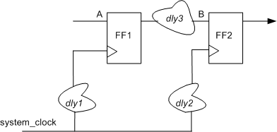
The digital circuit is shown with logic delay (dly3) and two clock buffer delays (dly1, dly2).
- How will you fix setup timing violations occurring at pin B?
- How will you fix hold violations occurring at pin B?
(Hint: Change the values of three delays to get desired effect)
Q.
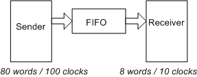
Sender sends data at the rate of 80 words / 100 clocks
Receiver can consume at the rate of 8 words / 10 clocks
Calculate the depth of FIFO so that no data is dropped.
Assumptions: There is no feedback or handshake mechanism. Occurrence of data in
that time period is guaranteed but exact place in those clock cycles is
indeterminate.
Q
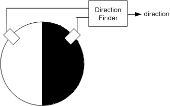
Optical sensors A and B are positioned at 90 degrees to each
other as shown in Figure. Half od the disc is white and remaining is black. When
black portion is under sensor it generates logic 0 and logic 1 when white
portion is under sensor.
Design Direction finder block using digital components (flip flops and gates) to
indicate speed. Logic 0 for clockwise and Logic 1 for counter clockwise.
Q
Will this design work satisfactorily?
Assumptions: thold = tsetup = tclock_out = tclock_skew = 1ns.
After reset A = 0, B = 1
Q. Design a 4:1 mux in Verilog.
- Multiple styles of coding. e.g.
- What are the advantages / disadvantages of each coding style shown above?
- How Synthesis tool will give result for above codes?
- What happens if default statement is removed in case statement?
- What happens if combination 11 and default statement is removed? (Hint Latch inference)
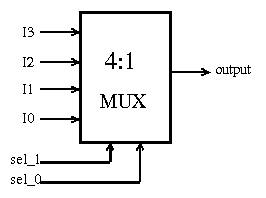
Using if-else statements
if(sel_1 == 0 && sel_0 == 0) output
= I0;
else if(sel_1 == 0 && sel_0 ==
1) output = I1;
else if(sel_1 == 1 && sel_0 ==
0) output = I2;
else if(sel_1 == 1 && sel_0 ==
1) output = I3;
Using case statement
case ({sel_1, sel_0})
00 : output
= I0;
01 : output
= I1;
10 : output
= I2;
11 : output
= I3;
default
: output = I0;
endcase
(Comments : Though this questions looks simple and out of text books, the answers to supporting questions can come only after some experience / experimentation.)
Q. Design a FSM (Finite State Machine) to detect a sequence 10110.
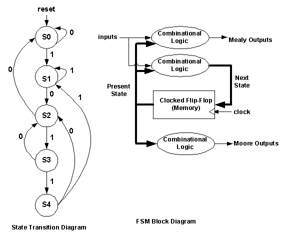
- Have a good approach to solve the design problem.
- Know the difference between Mealy, Moore, 1-Hot type of state encoding.
- Each state should have output transitions for all combinations of inputs.
- All states make transition to appropriate states and not to default if sequence is broken. e.g. S3 makes transition to S2 in example shown.
- Take help of FSM block diagram to write Verilog code.
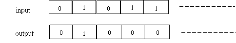
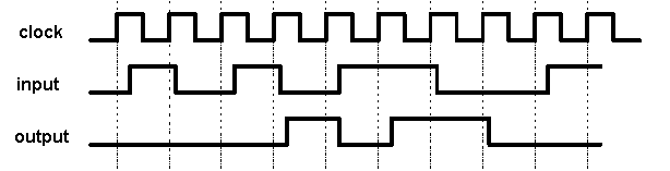
Q. One more sequence detector:
Design a FSM (Finite State Machine) to
detect more than one "1"s in last 3 samples.
For example: If the input sampled at clock
edges is 0 1 0 1 0 1 1 0 0 1
then output should be 0 0 0 1 0 1 1 1
0 0 as shown in timing diagram.
And yes, you have to design this FSM using not more than 4 states!!
Q. Design a state machine to divide the clock by 3/2.
(Hint: 2 FSMs working on posedge and negedge)
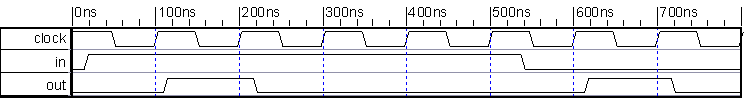
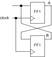
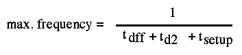
Q. Draw timing diagrams for following circuit.
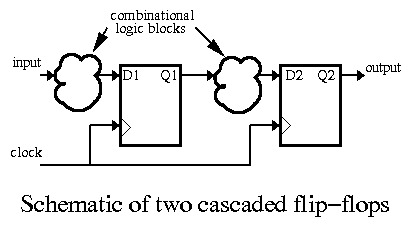
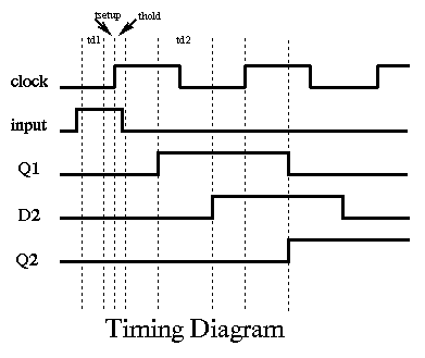
- What is the maximum frequency at which this circuit can operate?
- What is the minimum width of input pulse and position?
- Problem can be given interesting twist by specifying all delays in min and max types.
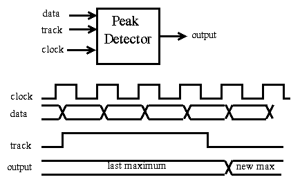
Q. Design a Digital Peak Detector in Verilog.
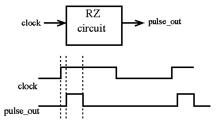
Q. Design a RZ (return to zero )circuit. Design a clock to pulse circuit in Verilog / hardware gates.
Q. Miscellaneous Basic Verilog Questions:
- What is the difference between Behavior modeling and RTL modeling?
- What is the benefit of using Behavior modeling style over RTL modeling?
- What is the difference between blocking assignments and non-blocking assignments ?
- How do you implement the bi-directional ports in Verilog HDL
- How to model inertial and transport delay using Verilog?
- How to synchronize control signals and data between two different clock domains?