|
Field Programmable Gate Arrays (FPGAs) --- Xilinx XC4000E Series
Much of the information below has been quoted from the current 4th Edition Xilinx Data Book. |
XC4000E Series SRAM FPGA Overview
The XC4000E family of high-performance, high-density Field Programmable Gate Arrays (FPGAs) provides the benefits of custom CMOS VLSI, while avoiding the initial cost, time delay, and inherent risk of a conventional masked gate array. The XC4000E family combines architectural versatility, on-chip Select-RAM memory with edge-triggered and dual-port modes, increased speed, abundant routing resources, and new, sophisticated software to achieve fully automated imple-mentation. The FPGAs are customized by loading configuration data into the internal memory cells. The FPGA can either actively read its configuration data out of external serial or byte-parallel PROM (master mode), or the configuration data can be written into the FPGA (slave and peripheral mode). The XC4000E family can run at synchronous system clock rates of up to 70 MHz and internal performance in excess of 150 MHz. Features
- Third Generation Field-Programmable Gate Arrays
- Select-RAM TM memory: on-chip ultra-fast RAM with - synchronous write option - dual-port RAM option
- Fully PCI compliant
- Abundant flip-flops
- Flexible function generators
- Dedicated high-speed carry-propagation circuit
- Wide edge decoders (four per edge)
- Hierarchy of interconnect lines
- Internal 3-state bus capability
- 8 global low-skew clock or signal distribution network
- Flexible Array Architecture
- Programmable logic blocks and I/O blocks
- Programmable interconnects and wide decoders
- Sub-micron CMOS Process
- High-speed logic and Interconnect
- Low power consumption
- Systems-Oriented Features
- IEEE 1149.1-compatible boundary scan logic support
- Programmable output slew rate (2 modes)
- Programmable input pull-up or pull-down resistors
- 12-mA sink current per output
- 24-mA sink current per output pair
- Configured by Loading Binary File
- Unlimited reprogrammability
- Six programming modes
- Readback capability
- Backward Compatible with XC4000 Family
- XACTstep Development System runs on ‘386/’486/ Pentium-type PC, Sun-4, and Hewlett-Packard 700 series
- Interfaces to popular design environments including VIEWlogic, Mentor Graphics and OrCAD
- Fully automatic partitioning, placement and routing
- Interactive design editor for design optimization
- Unified Libraries, including 288 soft macros and 34 Relationally Placed Macros (RPMs)
- RAM/ROM compiler
The XC4000E family is supported by powerful and sophisticated software, covering every aspect of design from schematic or behavioral entry, floorplanning, simulation, automatic block placement and routing of interconnects, to the creation, downloading, and readback of the configura-tion bit stream. The Xilinx XC4000E family includes three major configurable elements: configurable logic blocks (CLBs), input/output blocks, and interconnects. The CLBs provide the functional elements for constructing user's logic. The IOBs provide the interface between the package pins and internal signal lines. The programmable interconnect resources provide routing paths to connect the inputs and outputs of the CLBs and IOBs onto the appropriate networks. Customized configuration is established by programming internal static memory cells that determine the logic functions and internal connections implemented in the FPGA.
Specifications
| Device |
XC4013E |
| Aproximate Gate Count |
13,000 |
| CLB Matrix |
24 x 24 |
| Number of CLBs |
567 |
| Number of Flip-Flops |
1,536 |
| Max. Decode Inputs per Side |
72 |
| Max. RAM Bits |
18,432 |
| Number of IOBs |
192 |
| Horizontal Longlines |
48 |
| TBUFs per Longlines |
26 |
| PROM Size (bits) |
247,960 |
|
|
|
|
Goto TOP
|
|
|
Configurable Logic Blocks (CLB)
The principle CLB elements are shown in
Figure 1. Each CLB contains a pair of flip-flops and two independent 4-input function generators. These function generators have a good deal of flexabilty as most combinatorial logic functions need less than four inputs. Thirteen CLB inputs and four CLB outputs provide access to the functional flip-flops. Configurable Logic Blocks implement most of the logic in an FPGA. The principal CLB elements are shown in Figure 1. Two 4-input function generators (F and G) offer unre-stricted versatility. Most combinatorial logic functions need four or fewer inputs. However, a third function generator (H) is provided. The H function generator has three inputs. One or both of these inputs can be the outputs of F and G; the other input(s) are from outside the CLB. The CLB can therefore implement certain functions of up to nine variables, like parity check or expandable-identity comparison of two sets of four inputs.
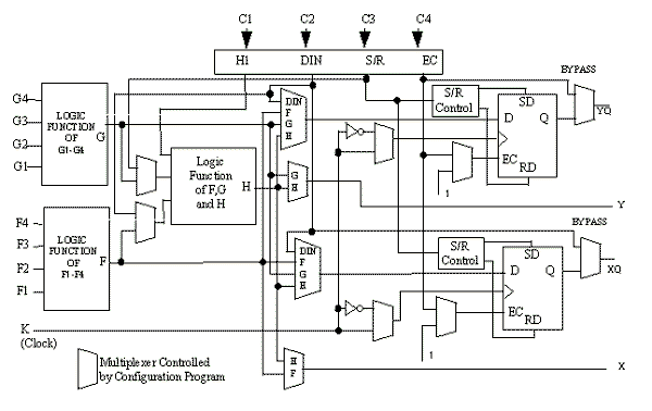
Fig. 1 Block Diagram of XC4000 Families Configuration Logic Block (CLB)
Each CLB contains two flip-flops that can be used to store the function generator outputs. However, the flip-flops and function generators can also be used independently. DIN can be used as a direct input to either of the two flip-flops. H1 can drive the other flip-flop through the H function gen-erator. Function generator outputs can also be accessed from outside the CLB, using two outputs independent of the flip-flop outputs. This versatility increases logic density and simplifies routing. Thirteen CLB inputs and four CLB outputs provide access to the function generators and flip-flops. These inputs and outputs connect to the programmable interconnect resources outside the block.
Four independent inputs are provided to each of two func-tion generators (F1 - F4 and G1 - G4). These function gen-erators, whose outputs are labeled F’ and G’, are each capable of implementing any arbitrarily defined Boolean function of four inputs. The function generators are imple-mented as memory look-up tables. The propagation delay is therefore independent of the function implemented. A third function generator, labeled H’, can implement any Boolean function of its three inputs. Two of these inputs can optionally be the F’ and G’ functional generator out-puts. Alternatively, one or both of these inputs can come from outside the CLB (H2, H0). The third input must come from outside the block (H1).
Signals from the function generators can exit the CLB on two outputs. F’ or H’ can be connected to the X output. G’ or H’ can be connected to the Y output. A CLB can be used to implement any of the following functions:
- any function of up to four variables, plus any second function of up to four unrelated variables, plus any third function of up to three unrelated variables
- any single function of five variables
- any function of four variables together with some functions of six variables
- some functions of up to nine variables
Implementing wide functions in a single block reduces both the number of blocks required and the delay in the signal path, achieving both increased density and speed. The versatility of the CLB function generators significantly improves system speed. In addition, the design-software tools can deal with each function generator independently. This flexibility improves cell usage.
The flexabilty and symmetry of the CLB architecture facilitates the placement and routing of a given application. Since the function generators and flip-flops have independent inputs and outputs, each can be treated as a seperate entity during placement to achieve high packing density. Inputs, outputs and the functions themselves can freely swap positions within thew CLB to avoid routing congestion during the placement and routing operation.
|
|
|
|
Goto TOP
|
|
|
Fast Carry Logic within the CLB
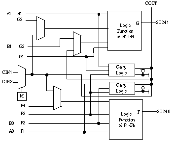 Fig. 2 Fast Carry Logic in Each CLB Fig. 2 Fast Carry Logic in Each CLB
Each CLB F and G function generator contains dedicated arithmetic logic for the fast generation of carry and borrow signals. This extra output is passed on to the next CLB function generator above or below. The carry chain is independent of normal routing resources. Dedicated fast carry logic greatly increases the efficiency and performance of adders, subtracters, accumulators, comparators and counters (Figure 2).The two 4-input function generators can be configured as a 2-bit adder with built-in hidden carry that can be expanded to any length. This dedicated carry circuitry is so fast and efficient that conventional speed-up methods like carry generate/propagate are meaningless even at the 16-bit level, and of marginal benefit at the 32-bit level.
|
|
|
|
Goto TOP
|
|
|
On-Chip Memory
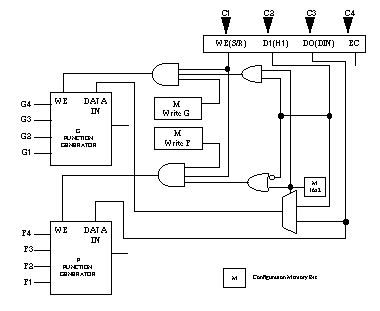 Fig. 3 CLB Function Generators can be used as Read/Write Memory Cells
RAM Configuration Options --- The function generators in any CLB can be configured as RAM arrays in the following sizes: 1) Two 16x1 RAMs: two data inputs and two data outputs with identical or, if preferred, different addressing for each RAM 2) One 32x1 RAM: one data input and one data output. One F or G function generator can be configured as a 16x1 RAM while the other function generators are used to imple-ment any function of up to 5 inputs.
Additionally, the XC4000E RAM may have either of two timing modes: 1) Edge-Triggered (Synchronous): data written by the designated edge of the CLB clock. WE acts as a true clock enable. 2) Level-Sensitive: an external WE signal must be supplied asynchronously.
The selected timing mode applies to both function generators within a CLB when both are configured as RAM. The number of read ports is also programmable: 1) Single Port: each function generator has a read port a write port; 2) Dual Port: both function generators are configured as a single 16x1 dual-port RAM with one write port and two ports. Simultaneous read and write operations to the same or different addresses are supported.
RAM Inputs and Outputs --- The F1-F4 and G1-G4 inputs to the function generators act as address lines, selecting a particular memory cell in each look-up table. The functionality of the CLB control signals changes when the function generators are configured as RAM. The DIN/ H2, H1, and SR/H0 lines become the two data inputs (D0, D1) and the Write Enable (WE) input for the 16x2 memory. When the 32x1 configuration is selected, D1 acts as the fifth address bit and D0 is the data input. The contents of the memory cell(s) being addressed are available at the F’ and G’ function-generator outputs. They can exit the CLB through its X and Y outputs, or can be captured in the CLB flip-flop(s). Configuring the CLB function generators as Read/Write memory does not affect the functionality of the other portions of the CLB, with the exception of the redefinition of the control signals. The H’ function generator can be used to implement Boolean functions of F’, G’, and D1, and the D flip-flops can latch the F’, G’, H’, or D0 signals.
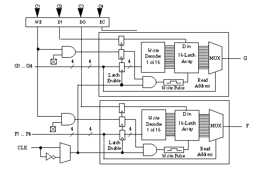
Fig. 4 16x2 (or 16x1) Edge-Triggered Single-Port RAM
Single-Port Edge-Triggered Mode --- Edge-triggered RAM simplifies timing requirements. The XC4000E edge-triggered RAM timing operates like writing to a data register. Data and address are presented. The register is enabled for writing by a logic High on the write enable input, WE. Careful timing relationships between address, data, and write enable signals are not required, and the external write enable pulse becomes a simple clock enable. The rising edge of WCLK latches the address, input data, and WE sig-and nals. An internal write pulse is generated that performs the write. See
Figure 4 for block diagram of a CLB configured as 16x2 (or 16x1) Edge-Triggered Single-Port RAM and
Figure 5 for block diagram of a CLB configured as 16x2(or 16x1) Edge-Triggered Dual-Port RAM.
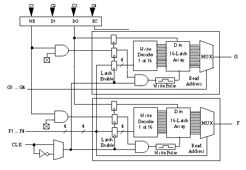
Fig. 5 16x2 (or16x1) Edge-Triggered Dual-Port RAM
|
|
|
|
Goto TOP
|
|
|
Input/Output Block
User-configurable input/output blocks (IOBs) provide the interface between external package pins and the internal logic. Each IOB controls one package pin and can be defined for input, output, or bidirectional signals. Figure 6 shows a simplified block diagram of the XC4000E IOB.
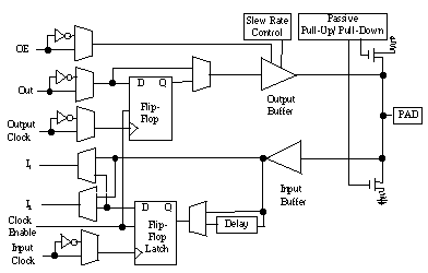 Fig. 6 Input/Out Block Fig. 6 Input/Out Block
Input Signals
Two paths, labeled I1 and I2, bring input signals into the array. Inputs also connect to an input register that can be programmed as either an edge-triggered flip-flop or a level-sensitive transparent-Low latch. The choice is made by placing the appropriate primitive from the symbol library.The inputs can be globally configured for either TTL (1.2V) or CMOS (2.5V) thresholds.
The two global adjustments of input threshold and output level are independent of each other. There is a slight hysteresis of about 300mV.Seperate clock signals are provided for the input and output registers; these clocks can be inverted, generating either falling-edge or rising-edge triggered flip-flops. As is the case with the CLB registers, a global set/reset signal can be used to set or clear the input and output registers whenever the RESET net is alive.
Registered Inputs
The I1 and I2 signals that exit the block can each carry either the direct or registered input signal. The input and output storage elements in each IOB have a common clock enable input, which through configuration can be activated individually for the input or output flip-flop or both. This clock enable operates exactly like the EC pin on the XC4000E CLB. It cannot be inverted within the IOB.
|
|
|
|
Goto TOP
|
|
|
Programmable Interconnects
All internal connections are composed of metal segments with programmable switching points to implement the desired routing. An abundance of different routing resources is provided to acheive efficient automated routing. The number of routing channels is scaled to the size of the array; i.e. it increases with the array size. The CLB inputs and outputs are distributed on all four sides of the block, providing additional routing flexibilty (Figure 7).
There are four main types of interconnect, three are distinguished by the relative length of their segments: single-length lines, double-length lines and Longlines. (NOTE: The number of routing channels shown in the figure below are for illustration purposes only; the actual number of routing channels varies with the array size.) In addition, eight global buffers drive fast, low-skew nets most often used for clocks or global control signals.
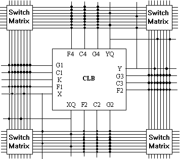
Fig. 7 Single-Length Lines
The single-length lines are a grid of horizontal and vertical lines that intersect at a Switch Matrix between each block.
Figure 7 illustrates the single-length interconnect surrounding one CLB in the array. Each Switch Matrix consists of programmable n-channel pass transistors used to establish connections bewteen the single-length lines. For example, a signal entering on the right side of the Switch Matrix can be routed to a single-length line on the top, left or bottom sides, or any combination thereof. Single-length lines are normally used to conduct signals within a localized area and to provide the branching for nets with fanout greater than one.
The function generator and control inputs to the CLB (F1-F4, G1-G4, and C1-C4) can be driven from any adjacent single-length line segment. The CLB clock (K) input can be driven from one-half of the adjacent single-length lines. Each CLB output can drive several of the single-length lines, with connections to both the horizontal and vertical Longlines.
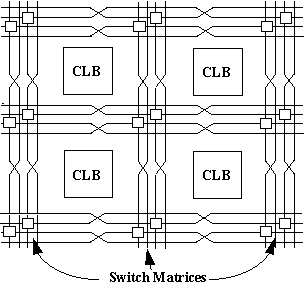
Fig. 8 Double-Length Lines
The doubled-length lines (Figure 8) consists of a gird of metal segments twice as long as the single-length lines; i.e. a double-length line runs past two CLBs before entering a Switch Matrix. Double-length lines are grouped in pairs with the Switch Matrices staggered so that each line goes through a Matrix Switch at every other CLB location in that row or column. As with single-length lines, all the CLB inputs except K can be driven from any adjacent double-length line, and each CLB output can be drive nearby double-length lines in both the vertical and horizontal planes. Double-length lines provide the most efficient implementation of intermediate lenggth, point-to-point interconnections.
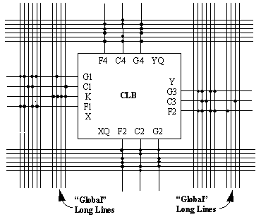 Fig. 9 Long-Line Routing Fig. 9 Long-Line Routing
Longlines form a grid of metal interconnect segments that run the entire length or width of the array (Figure 9). Additional vertical longlines can be driven by special global buffers, designed to distribute clocks and other high fanout control signals throughout the array with minimal skew. Longlines are intended for high fan-out, time-critical signal nets. Each Longline has a programmable splitter switch at its center, tat can seperate the line into two independent routing channels, each running half the width or height of the array. CLB inputs can be driven from a subset of the adjacent Longlines; CLB outputs are routed to the Longlines via a3-state buffers or the single-length interconnected lines.
|
|
|
|
Goto TOP
|
|
|
Wide Edge Decoders
Dedicated circuitry boosts the performance of wide decoding functions . When the address or data field is wider than the function generator inputs, FPGAs need multi-level decoding and are thus slower than PALs. XC4000E-family CLBs have nine inputs. Any decoder of up to nine inputs is, therefore, compact and fast. However, there is also a need for much wider decoders, especially for address decoding in large microprocessor systems. An XC4000E FPGA has four programmable decoders located on each edge of the device. The inputs to each decoder are any of the I1 signals on that edge plus one local interconnect per CLB row or column. Each decoder generates a High output (resistor pull-up) when the AND condition of the selected inputs, or their complements, is true. This is analogous to the AND term in typical PAL devices.
 Fig. 10 Wide Edge Decoder Fig. 10 Wide Edge Decoder
Figure 10 shows an example of edge decoding. Each row or column of CLBs provides up to three variables or their compliments. Each of these wired-AND gates is capable of accepting up to 72 inputs on the on the XC4013E. These decoders may also be split in two when a large number of narrower decoders are required, for a maximum of 32 decoders per device. The decoder outputs can drive CLB inputs, so they can be combined with other logic to form a PAL-like AND/OR structure. The decoder outputs can also be routed directly to the chip outputs. For fastest speed, the output should be on the same chip edge as the decoder. Very large PALs can be emulated by ORing the decoder outputs in a CLB. This decoding feature covers what has long been consid-ered a weakness of older FPGAs. Users often resorted to external PALs for simple but fast decoding functions.
|
|
|
|
Goto TOP
|
|
|
Links to More Information on Xilinx XC4000E Series FPGA
 Xilinx's XC4000 Product Infomation Xilinx's XC4000 Product Infomation
FPGA Product Selection Matrix
|
|
|
|
Goto TOP
|
(C) 1995-98 by Virtual Computer Corporation. All Rights Reserved. The names, logos and icons identifying VCC's products and services are proprietary marks of Virtual Computer Corporation.
|