Next: 6 Lessons Learned Up: Appnotes Index Previous:4 Integrated Toolset Example for COTS Architecture
![]()
![]()
![]()
![]()
Next: 6 Lessons Learned
Up: Appnotes Index
Previous:4 Integrated Toolset Example for COTS Architecture
The RASSP benchmark SAR generates a strip SAR map with a squint angle 90 degrees to the platform velocity vector. It covers a swath of 375 meters at a range of 7.26 K meters. The ADST radar is a fully polarimetric air- to- ground SAR. The radar transmit polarization alternates between horizontal polarity (H- pol) and vertical polarity (V- pol), while H- pol and V- pol are simultaneously processed in the receiver. The radar transmits at a 3kHz rate, so that the same- polarization pulse repetition frequency (PRF) is 1.5 kHz. The SAR resolution is 0.3 meters. The algorithm processes three transmit- receive polarization pairs: HH, VV, and either HV or VH.
For the RASSP benchmark, Lincoln Laboratories provided both an executable specification, written in VHDL, and a list of key system requirements. The system requirements for the RASSP SAR benchmark followed from its intended use to form images of the Earth surface from an airborne platform (Amber UAV) and use them for ATR. These requirements include:
Pulse Repetition Frequency: The physics of the radar transceiver and the system environment may determine the PRF (e.g. the distance to the target defines a minimum PRF).
Acceptable error from "gold" functional output: The RASSP benchmark executable specification developed by Lincoln Labs was delivered with test input data and the corresponding "gold" functional output. This information is essential for testing finite word length effects.
Acceptable latency: Latency for this algorithm is defined as the time from the input of the last pulse of a frame to the display of last row of the output image.
Acceptable utilization of hardware components: A system specification often defines some growth margins in terms of component utilization. Growth margins are an important factor in RASSP designs, since model- year upgrades can cause growth in processing loads.
Acceptable levels of memory occupancy: A system specification often defines some growth margins in terms of available memory. This is another growth margin that is important in RASSP systems where model- year upgrades are anticipated.
A key element of the LM- ATL RASSP design process which spans both the architecture process and the detailed design process is virtual prototyping. The various levels of the virtual prototype of the SAR system were used in a hierarchical fashion to quickly assess design risks involved in integrating the hardware and software elements and minimize or eliminate those risks. The first level of virtual prototype was a network performance model which used VHDL to describe data communications at the packet level transfer and modeled the application code with a pseudo- code which was interpreted by the computational element of the processor model. This allowed true hardware/software codesign with the independent specification of the software and hardware. Each of the candidate architectures was evaluated to ensure minimum system sizing (number of processors and amount of memory), and optimum software mapping, and to eliminate performance bottlenecks of the interprocessor communication network.
The second level of virtual prototype added functionality to the performance (timing and structure) models. A data field added to the network token allowed actual data passing between the models, and the high level pseudo- code modeling of the software running on the processors used in the performance simulation was replaced with processes making DSP math library calls.
The third level of virtual prototype described the custom modules down to individual components at the behavioral level with emphasis on interface behavior rather than internal chip structure, and described the FPGAs in synthesizeable VHDL at the RTL level. (Details of the performance modeling and virtual prototyping are found in the "Token- Based Performance Modeling" and "Virtual Prototyping Concepts" Application Notes.)
Processor behavioral and performance simulations using the VHDL virtual prototype support trade- offs. Mixed levels of simulation (algorithm, abstract behavioral, performance, ISA, RTL, etc.) are used to verify interaction of the hardware and software. These models are composed largely of hierarchical VHDL models of the architecture. We choose the models, to the maximum extent possible, from the MYA elements in the RASSP reuse library. The RASSP team develops and inserts new required library elements into the reuse library to support this design phase. The executable specification has now evolved into a more detailed set of functional and performance models that are architecture- specific. Software algorithm implementations are also now specific to the candidate architecture(s).
Lockheed Martin ATL evaluated two COTS- based hardware architectures for the RASSP SAR benchmark system both based on Mercury Raceway configurations. Mercury provides several processor options for its MCV6 system, including two considered in these Hardware/Software configuration tradeoffs: the Intel i860 processor, and the Analog Devices ADSP21062 SHARC processor. The two configurations considered were:
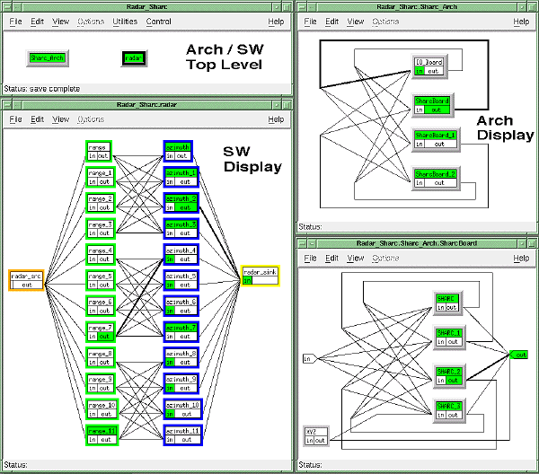
Example results of token- based performance modeling and simulation performed on a twelve (12) processor SHARC architecture are shown in Figures 5 - 2 and 5 - 3. Figure 5 - 2 shows a high level graphical depiction of the software corresponding to three polarizations of SAR processing and a graphical depiction of the hardware being simulated. The hardware view shows the top level architecture consisting of an I/O board and three Sharc boards. Each Sharc board is hierarchical and can be expanded as shown in the figure. The software view represents the processing in the form of a source of data, twelve identical range processing functions, twelve identical azimuth processing functions, and a data sink. The mapping of the algorithm is such that a range processing function and the corresponding azimuth processing function are mapped to one of the twelve SHARC processors in the architecture. The interconnections between four range functions and four azimuth functions represents a distributed corner turn which is necessary due to the size of the images being processed and the limited memory associated with each processor. The three interconnected groups of range and azimuth functions represents identical processing for the three polarizations required.
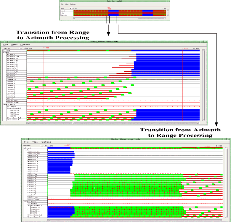
Figure 5 - 3 shows the top level view of the simulation results in the form of a timeline, along with two expanded views corresponding to interesting transition areas. In each expanded timeline there is a line corresponding to each of the twelve range and azimuth functions in the software graph as well as the source and sink functions. There is also one line for the I/O board and the three SHARC boards, with one of the SHARC boards expanded to show the four individual SHARC processors. The images in Figures 5 - 2 and 5 - 3 are created using the Architecture Definition and Visualization Tool (ADVT) which also provides the ability to "replay" the simulation on the graphical representations of the hardware and software for analysis purposes. The simulation was performed using VHDL and the simulator output postprocessed for insertion into ADVT. The highlighted inputs or outputs on either the hardware or software graph in Figure 5 - 2 indicates that a data transfer is in process or pending. A highlighted title bar indicates that the particular software process is active or the architecture resource is busy. A highlighted connection indicates that data communication is in progress.
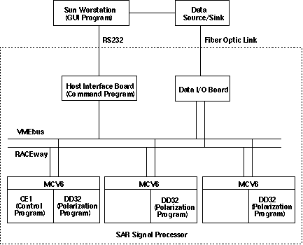
The LM- ATL selected SAR signal processor architecture, shown in Figure 5 - 4, contains four major architectural elements:
Mercury Computer Systems MCV6 Processor Boards (VME 6U format) perform the bulk of the signal processing. Each MCV6 can have up to two daughtercards. The SAR signal processor design uses a single daughtercard containing four Analog Devices ADSP21062 SHARC processor chips with 32 MBytes of DRAM for the processing of each polarization.
A 68040 based single board computer (SBC), the Motorola MVME162, serves as the host interface and controls the SAR signal processor operation. When the SAR signal processor is in stand- alone mode, the 68040 boots the SAR signal processor and controls its operation.
A custom designed Data I/O Board interfaces the SAR signal processor to the radar data source and sink, and performs front end signal processing functions. This includes synchronizing operation based upon the preamble sent with each pulse, performing video- to- baseband I/Q conversion, FIR filtering, and keeping track of pulse, polarization, and frame boundaries.
An interconnect network consisting of Mercury Computer Systems Raceway acts as a high- bandwidth, point- to- point network for data transfer, and the VMEbus performs control operations.
The main risk with the chosen architecture was that the ADSP21062 SHARC processors were not yet available when the choice was made. Therefore, a risk mitigation plan was established to use dual i860 daughtercards for the signal processing if the SHARC based daughtercards were not available at the time of system integration. A single polarization design requires two i860 boards, each with two daughtercards, and a three polarization design requires five i860 boards, each with two daughtercards. Because of SHARC processor unavailability in the time remaining for iimplementation prior to the Second Annual RASSP Conference, a single polarization, I860 based architecture was developed.
Software development in the architecture process deviates significantly from traditional approaches. The functionality which has been allocated to software can be broken into three major areas:
This is accomplished using a graph- based programming approach(es) that supports correct- by- construction software development based on algorithm and architecture- specific support library elements.
Mangement Communications and Control Inc (MCCI), a Lockheed Martin ATL RASSP subcontractor has developed an autocoding system which generates the software automatically from the PGM data flow graph description. The autocoding process is driven from:
The autocoded graph partitions are executed under the control of a Static Run- Time System which provides graph management facilities, a reusable interprocessor communication substrate, and a well defined external interface for control.
The third major process is the detailed design of software and hardware elements. As with the system and architecture processes, detailed design is carried out and verified for both hardware and software via a set of detailed functional and performance simulations. At the completion of this process, the design is established.
The RASSP software development methodology was used to develop the SAR benchmark, but since the RASSP autocoding tools were not yet available, the SAR application software had to be hand coded. Subsequent to completion of the hand coding, the MCCI autocode tool was completed and delivered to ATL. In order to exercise the tool, it was used to reimplement the application software portion of the SAR problem. The results of this exercise were very impressive.The Autocode Tools truly output a complete solution. Loading and starting the processes was performed flawlessly by the tool. In addition, all memory management and interprocessor communications is included in the generated code. It is important to note that all interprocessor communication was provided by the Run- Time System and that the application developer had to write no communication software to achieve correct interprocessor communication the first time. This exercise was the first time the RASSP software methodology was demonstrated. Overall, the exercise was a success and marked a major milestone for the RASSP program.
The exercise lasted approximately one month. After generating the required PGM graphs, the tools automatically generated all code necessary to implement the graphs on the target hardware. The only thing which needed to be hand coded was the IO Procedure which interfaced the application graph to the ATL designed IO Board. The tool provides a set of library services to support the IO Procedure to application graph interface. System integration took approximately 2 weeks. This is significantly less time than was required to integrate and test the hand coded software. The autocoded software's execution efficiency was within 15% of the hand coded software. Although memory efficiency was not as good, a number of areas were identified and subsequently improved.
During the hardware portion of the detailed design process, behavioral specifications of the processor are transformed into detailed designs (RTL and/or logic- level) through a combination of hardware partitioning, parts selection, and synthesis. Detailed designs are functionally verified using integrated simulators, and performance/timing is also verified to ensure proper performance. The process results in detailed hardware layouts and artwork, net lists, and test vectors which can then be seamlessly transitioned to manufacturing and test via format conversion of the data.
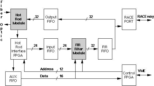
The hardware design for the SAR signal processor consisted of the mechanical design of the chassis and the design of the data I/O Board. All other boards in the SAR signal processor are off the shelf modules which required no new hardware design. Hence, the hardware design discussion focuses on design of the Data I/O Board shown in block diagram form in Figure 5 - 5.
The Hot Rod module (HRC- 500FS Fiber Optic Interface Card) provides separate fiber optic interfaces for the input radar data and output image data. The Hot Rod daughtercard interfaces to the rest of the Data I/O Board through two 40- bit wide buses - one for transmit and one for receive. The input data rate of 4.56 Megawords and output data rate of 6.83 Megawords are both within the 11.25 Megawords maximum of the Hot Rod. The Hot Rod has an internal loopback mode that connects the transmit side back to the receive side. The loopback mode is used during Data I/O Board
The Hot Rod Interface FPGA performs a number of operations on the radar data in addition to controlling the Hot Rod. The Hot Rod Interface FPGA contains logic that looks for the preamble that defines the beginning of a radar pulse. Once the start of a pulse is detected, the odd and even data samples are extracted along with bit serial data defining polarization and auxiliary radar data. The 12- bit odd and even pulse samples are modulated by (- 1)n before being written into the Input FIFO. The auxiliary radar data is written to the AUX FIFO. The number of words, pulses, and image frames in both the receive and transmit channels are counted as part of the I/O control.
The FIR filter daughtercard is capable of simultaneously processing I and Q channel data at a 5 MHz input rate. The input data is 12- bit twos complement, the filter coefficients are 23- bit twos complement, and the output is 32- bit twos complement in both I and Q. Each channel uses two Plessey PDSP16256 Programmable FIR Filter chips configurable with up to 64 taps, with one FIR chip processing the most significant portion of the filter coefficients, and the other processing the less significant portion of the filter coefficients. The 16K deep FIR FIFO buffers received data until it is sent out of the RACE interface.
The RACE port interface contains two ASICs designed by Mercury Computer Systems, Inc. The RACE interface sends the received radar data to the appropriate signal processor, and receives output image data from the signal processors. The 4k- deep output FIFO provides data buffering between the RACE interface and the Hot Rod transmit port.
The Control FPGA controls the operation of the FIR filter and the FIFOs, keeps track of the status of all FIFOs, and implements the VMEbus interface.
Test considerations played an important part in the design of the Data I/O Board and associated FPGAs. One testability issue is the lack of JTAG scan on a majority of the COTS components. The design approach taken was to add JTAG scan bus transceivers to signal paths between non- JTAG devices. A second testability issue is the presence of asynchronous interfaces. The approach taken is to design these interfaces so that they can be tested synchronously, and to add test modes that force synchronous operation. Test modes included in the FPGA design enable bypass of either the PRI detection logic or the FIR Filter. FIR bypass is significant in that it allows testing of the Data I/O motherboard without the FIR Filter daughterboard in place. FPGA test modes reduce the cycle time of high modulo counters, allowing testing of higher order counter bits. The various test modes, which are part of the VHDL model, are included in the data I/O functional simulations.
Synopsys was used to synthesize logic for the two FPGAs using the AT&T ORCA cell library. NeoCAD was then used to map these cells to the ATT2C15 FPGA programmable logic cells (PLCs), place the cells, and route the interconnect between the cells. Static timing analysis (using NeoCAD) after mapping, placement, and routing was performed to identify any nets not meeting timing and speed specifications. In some cases, it was necessary to go back and modify the VHDL description to meet timing and speed specifications. A typical modification was the introduction of pipelining on paths not meeting speed. Once the FPGA design was completed, the logic and timing was back- annotated into the board level VHDL model and functionality was reverified.
Detailed schematics of the Data I/O Board design were captured using Mentor Graphics Design Architect. The schematics could not be finished until the FPGA design was completed with all pin assignments finalized. Once the schematics were finalized, placement and routing using Mentor Boardstation were performed for the Data I/O motherboard and FIR filter daughterboard. The board layout parasitics were back- annotated into the VHDL model to confirm that functional and timing specifications are met.
Since most of the software developments are verified during the architecture phase, they are limited at this point to generation of those elements that are target- specific. This includes configuration files, bootstrap and download code, target- specific test code, etc. All the software is compiled and verified (to the extent possible) on the final virtual prototype prior to the detailed design review. Design release to manufacturing marks the end of the RASSP design process.
5.0 Hardware / Software Codesign Process Applied to Mixed COTS / Custom Architecture
5.1 SAR Benchmark Application
The RASSP SAR algorithm provides high- resolution, all weather images that can be used to identify main- made objects that are on the ground or in the air. Such object identification typically requires SAR processing to be performed in real- time by means of an embedded signal processor. This application is based on the MIT Lincoln Laboratory Advanced Detection Technology Sensor (ADTS), which is a Ka band SAR (33.56 GHz) sensor. The ADST system consists of an integrated radar, navigation, and recording system. The form factor for the RASSP SAR processor is consistent with operation on board the Amber Unmanned Autonomous Vehicle (UAV).
5.2 Application of Hardware / Software Codesign
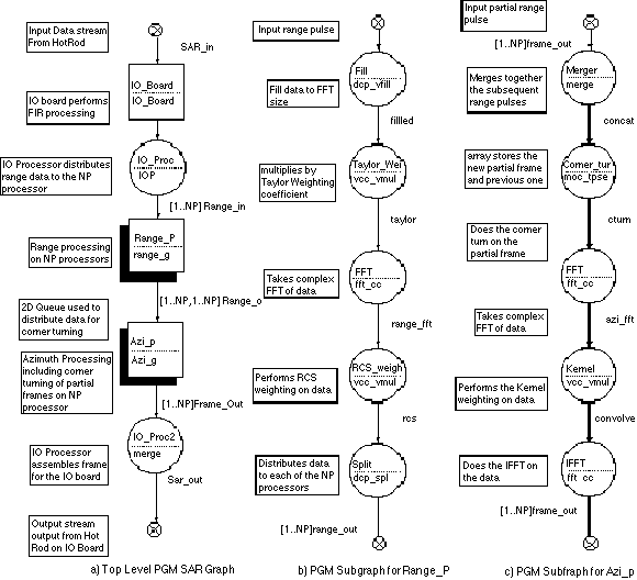
The SAR application in the Processing Graph Method (PGM) notation is shown in Figure 5 - 1a. The radar data stream is received by the IO_Board in a series of 512 sequential range pulses of 2032 complex numbers. Each range pulse is FIR filtered by the IO Board and then a separate IO process distributes each subsequent pulse to NP processes. This is repeated for all of the 512 pulses in each image frame. The range processing which is defined in the Range subgraph in Figure 5 - 1b proceeds for each of the NP range. At the end of the range processing the range pulse is divided into NP segments and each of the NP - 1 segments are sent to the appropriate azimuth processes. The PGM mechanism that represents this data distribution process is a two dimensional family queue indicated on the figure as [1..NP,1..NP]Range_o. Families are noted in PGM by the shaded nodes. The data from the range processing is loaded into one of the dimensions of the queue associated with that range family. There are NP of these one dimensional queues for a total of 2 * NP queues which are represented by the two dimensional family shown in Figure 5 - 1a. The azimuth process first merges the data from the NP queues. The data is then corner turned and the azimuth processing shown in Figure 5 - 1c is completed on this partial data set. After each partial azimuth frame is completed the IO process (IO_Proc2) moves these partial frames sequentially back to the IO board.
![]()
![]()
![]()
![]()
Next: 6 Lessons Learned
Up: Appnotes Index
Previous:4 Integrated Toolset Example for COTS Architecture