Department of Electrical Engineering
University of Edinburgh
The King's Buildings
Edinburgh, EH9 3JL
Scotland, UK
ABSTRACT
This paper describes a single-chip, bit-serial correlator design for Spread-Spectrum applications. The device has an input data word of 4-bits which is correlated with 512 binary taps and operates at a sample rate of 2.4MHz (typical) producing a full-precision 13-bit sum. The internal architecture is bit-serial, and is driven by a clock (30MHz) derived from the external sample clock using the internal clock distribution network as a ring oscillator. The techniques are described which overcome the problems of clock-skew in this design.
This bit-serial correlator forms the basis of a Spread Spectrum Communication Receiver which correlates received data with a pseudo-random code word. The architecture includes a cascade of bit-serial adders whose design is made simple by using a ones-complement numbering system with a shifted zero. This strategy removes the need for control signals or their associated distribution networks to the adder units.
The design also demostrates a new clocking strategy which relies upon the generation of an internal clock using its own distribution network as a ring-oscillator. The external clock signal is used to latch bit-parallel data across the component boundaries, and to initiate the internal clock which drives the internal bit-serial architecture. The clock distribution network itself drives a synchronous design with over 3.5K bit-registers distributed throughout a 70 mm-sq component.
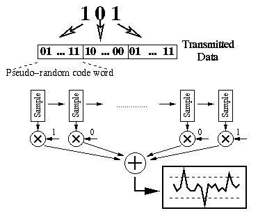
Spread Spectrum Communication relies upon expanding each bit of data into a sequence of transmitted data which can be detected with greater reliability against noise in the communication channel. Typically the code word is the maximal length sequence of an irreducible polynomial. As shown in Figure 1, the message data is translated bit by bit into the codeword (for 1 say) or its complement (for 0), and transmitted. The receiver is a correlator which matches the sample data stream against the codeword and the output function will deviate significantly from a base value due to random noise, only when the transmitted codeword aligns exactly.
The communication channel is an analog medium. The sampled data can be converted to digital into m-bits. If m=1, then the correlation can be implemented by simply counting matches, and a match is deemed to have occurred if there is either a very large or a very small number of matches. This thresholding, however, has large loss in Gaussian noise which can be reduced by increasing the digital range. If m>1, then the correlation can be implemented with a full sum as described below. In this case, the thresholds depend also upon the mapping of the analog to the digital range. For this design, the correlation takes 4-bit sampled data with a codeword of 512 (or optionally 511) bits in length.
There are two aspects of the arithmetic which must be highlighted: 1) weighting is achieved by simply bit-complementing the data and using only positive integer arithmetic, and 2) the adder cascade is achieved without control signals by "zero-stuffing" the redundant bits of the data stream.
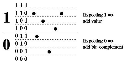
The aim of the correlation function is to determine whether the current 512, 4-bit samples match the expected codeword. This is achieved by a weighted summation of the samples where the weights are the binary code bits and the weighting is performed by complementing the data bits when a zero is expected. Figure 2 illustrates this for a 3-bit digital sample. The analog to digital conversion is set such that the average value of the incoming signal is in the centre of the digital range and so the expected sum, for random inputs, is 512 * 3.5. When a zero is expected, the weighting effectively reflects the digital range through the "average" value so that a low sample value is transformed into a high weighted value and visca-versa. If a one is expected, the weighting passes the value unchanged. Thus deviation from the expected sum indicates the degree of correlation or anti-correlation (as illustrated in Figure 1).
The basic architecture is shown in Figure 3. The sample data is converted to parallel form and shifted through the 512, 4-bit tap data-registers. The adder cascade consists of 9 layers of bit-serial adder units, each taking the output of two units from the previous layer and feeding its output to the following one. Thus the first layer has 256 adder units, the next 128, and so on to the final layer of a single unit producing the total summation in bit-serial form.
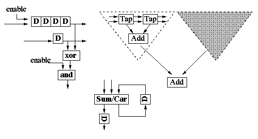
Clearly the sum of two n-bit numbers is (n+1)-bits which, in a bit-serial architecture, implies that the output sequence of the sum is longer by one clock cycle. Thus the original four-bit inputs to the first layer become five-bit inputs to the second; and, finally, 13-bit outputs form the 9th layer. Thus, for each input date sample, a 13-bit word is generated which leads to an internal word cycle of 13 bit-clocks.
The need for control signals to the adder units (to signify word boundaries) is avoided by stuffing the non-significant bits of the 13-bit word with zeros. In the tap units, the sample data word is shifted for the first 4 bit-cycles of each 13-bit word cycle; for the remaining 9 bit-cycles, the sample word is held and the output of each tap is low (or zero) as in Figure 3. At each adder unit, if the value following the most significant bit is zero on both inputs then the output is the previous carry and the carry register is cleared:
and the output and carry are zero thereafter so long as both the inputs remain so. Thus the zero-stuffing of non-precision bits is maintained throughout the array.
As levels of integration increase, so too does the relative capacitance on the clock signal line due to larger numbers of state elements on a single component. Appropriate clock buffering can minimize the resulting delay[1] but high current and transmission line effects require distributed buffering[2]. This leads to independent nodes in the clock distribution network and the possible danger of clock-skew due to imbalanced propagation paths. While a multiphase clocking scheme reduces this problem[3], a single phased clocking scheme offers the advantages of a simpler design style and reduced routing overheads[4].
There are over 3.5K single clock-edged D-types in this component which must be driven by the bit-clock. This is achieved by a combination of: 1) distributing the clock signal in the opposite direction to the data flow, 2) balanced placement and buffering of the clock distribution buffers within the adder cascade. These techniques together overcome the clock-skew problems, and the former also reduces spikes on the power and ground supplies since the design is not clocked simultaneously.
For each sample cycle, there are thirteen internal bit cycles to drive the bit serial arithmetic. These are generated using the full clock distribution network as a feedback loop, with control circuitry to count and terminate the bit-clock cycles. The main advantages are:
On the rising of the external sample (or word) clock signal, the control logic completes the feed-back loop of the internal bit-clock distribution network and initiates the bit-clock signal. At the end of the internal word cycle, the control logic is reset, and the feed-back loop broken, by a 13-cycle counter. To facilitate testing and timing analysis, and to provide a signal for possible hand-shaking protocols, an external output indicates when the internal logic has completed processing the previous sample. At this stage, the internal logic is held until the sample clock signal is next raised.
The resulting component is 70mm-sq in a 1.2µ 2-metal CMOS process, and performs a full-precision binary-weighted summation on 512, 4-bit words at a typical sample rate of 2.4MHz with an internal (self-generating) clock speed of 30MHz.
This paper has presented the architecture of a highly integrated correlator design for Spread Spectrum Communications, with the important features of: