Abstract: This correspondence reexamines the design by Srinivas and Parhi[1] which used redundant-number adders for fast twos-complement addition. The underlying mechanism is revealed and improvements are presented which lead to a static-logic binary-tree carry generator to support high-speed adder implementations with a delay of |log2(N)|+2 gates.
In 1992, Srinivas and Parhi[1] presented a design for a twos-complement adder which uses Signed Redundant Number Representation[2] (SBNR). Since conventional binary is a subset of SBNR, two n-bit twos-complement numbers {aN-1...a0} and {bN-1...b0} can be summed as SBNR numbers (without carry propagation) to yield an N-digit SBNR number. The Srinivas and Parhi architecture consisted of such an addition stage and followed by conversion of the SBNR sum back into twos-complement format. The authors claimed that this provided the fastest architecture for the addition of two twos-complement numbers.
However, the initial SBNR addition block of [1] can be replaced by xor(ai,bi), xnor(ai,bi) and and(ai,bi) (conventional propagate and generate signals for a carry-lookahead adder); and the remaining circuit can thus operate directly on twos-complement representation producing the inverse of the sum (easily corrected). With trivial changes, we can also use nand(ai,bi) instead of and(ai,bi) and so reduce the gate count of the design by 3N-1 and the critical path by 2. More significantly, the design is thus equivalent to our hybrid carry-lookahead / carry-select architecture shown in Fig. 1 and it is a purely twos-complement architecture whose high speed has no reliance upon SBNR.
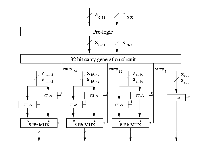
In Fig. 1 (which corresponds to Fig. 6 and 8 in [1]), the pairs of 8-bit additions are performed using carry-lookahead logic and their outputs selected according to the true value of the corresponding carry-in. Unlike the usual carry-select architecture[3], the carry terms are generated by independent logic rather than by using the results of successive adder sub-sections; this is where the speed advantage lies since the Srinivas and Parhi design uses a tree structure to achieve O(log(N)) delay.
The carry-generator is based on a novel 8-digit SBNR sign-checking circuit presented in [1] (Fig. 7 in [1]). There are two inputs to the circuit {ZN-1,...Z0} and {SN-1,...S0} which in [1] are generated by manipulation on an SBNR sum and interpreted as zero and sign. We have replaced this pre-logic with Zi=xor(ai,bi) and Si=and(ai,bi), and the remainder of the circuit can be described in the following way. Define Zj,k=and(Zj,Zj-1,...Zk+1,Zk), and Cj,k as the carryOut of the addition of bits j through to k with a zero carryIn (giving Cj,j=Sj).
We build a carry-generator tree using the following relations at each node:
nand(Zp,q,Zr,p-1)=Zr,q
nor(Zp,q,Zr,p-1)=Zr,q
which effectively combines two adjacent adder sections. The first relation states that the carryOut of combined sections is the same as the carryOut of the more significant section unless its inputs are such that its carryIn propagates through it completely. This is so when each bit has a "0" and a "1" input and the resulting carryOut will then be the carryOut of the less significant section. (In practice we propagate carry to use an initial nand to form Sj.) The second and third relations maintain the function each bit has a "0" and a "1" input for the combined inputs at each node; these two relationships are not needed at the leaf nodes.
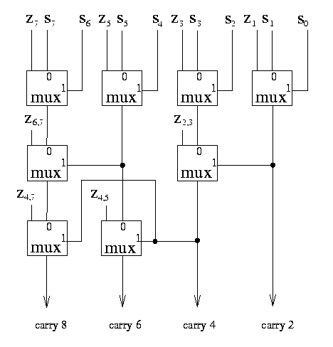
By applying these relations first to pairs of inputs, and then to pairs of the outputs of such pairs, etc, we build up a simple binary tree. This naturally produces carryOut on boundaries for successive powers of 2 (2, 4, 8, 16 etc); to obtain carryOut on intermediate boundaries, we augment the tree with other nodes (using the same relationship). Fig. 2 shows this for a 8-bit carry generation tree with 2-bit boundaries. Note that the generation of carry-bit 6 from inside the tree structure shows how the critical delay on each term can be limited to |log2(N)|. We believe this was not known to Srinivas and Parhi since it allows the use of 4-bit adder sections in their 32-bit example which moves the critical path from the carry-lookahead adders to the carry-generate tree and thus would have reduced their critical path delay.
The optimal decomposition for this architecture is found by determining the delay through the binary-tree carry generator and then selecting adder sub-sections (not necessarily carry-lookahead) which complete within that time. The only problem is fan-out, but this will be constrained in practice since larger adder tree sizes will lead to larger carry-boundaries.
The carry-generator tree is based upon two-input gates and multiplexors and, we believe, is suitable for the implementation of large adders using circuit techniques such as complementary pass-transistor logic[4] (CPL) which provide both high speed and low power. With the improvements outlined above, this circuit technique leads to a critical path delay of |log2(N)|+2 gates. Thus a 32-bit adder, with a sub-block size of 4-bits, will have a critical path of 7 gate delays, compared to 12 as reported in [1].
The underlying architecture can now be seen to be similar to that of Lynch and Swartzlander[5] also published in 1992. Their design creates a tree structure using 4-input dynamic-logic Manchester carry chains and uses ripple adders in place of the carry-lookahead adders. Like Srinivas and Parhi their "modified" tree produces carry signals only on 8-bit boundaries. In contrast, the design presented here provides a simple static-logic implementation based on two-input nodes with greater flexibility in choosing the carry boundaries and with no requirement for a system clock. Our design also has similar performance to that reported by Suzuki et al [6] but with fewer gates. Finally, we also note that our improved circuit can form the basis for a fast SBNR to twos-complement conversion.
We have revealed the true source of the speed advantage in the Srinivas and Parhi[1] design, and have reduced the number of gates by 3N-1 and the critical path to |log2(N)|+2 gate delays.